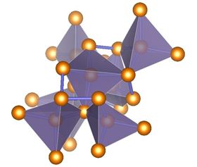
 This is an illustration of ST12-germanium's complex tetragonal structure with tetrahedral bonding. Image: Haidong Zhang.
Germanium may not be a household name like silicon, its group-mate on the periodic table, but it shows great potential for use in next-generation electronics and energy technology.
Of particular interest are forms of germanium that can be synthesized in the lab under extreme pressure conditions. So far, however, one of the most-promising forms of germanium for practical applications, called ST12, has only been created in tiny sample sizes – too small to confirm its properties definitively.
"Attempts to experimentally or theoretically pin down ST12-germanium's characteristics produced extremely varied results, especially in terms of its electrical conductivity," said Zhisheng Zhao from the Carnegie Institution and member of a research team that set out to study this form of germanium.
Led by Carnegie's Timothy Strobel, this research team was able to create ST12-germanium in a large enough sample size to confirm its characteristics and useful properties. The team reports its findings in a paper in Nature Communications.
"This work will be of interest to a broad range of readers in the field of materials science, physics, chemistry and engineering," explained Carnegie's Haidong Zhang, the co-leading author of the paper.
ST12-germanium has a tetragonal structure – the name ST12 means ‘simple tetragonal with 12 atoms’. The team created it by exposing germanium to about 138 times normal atmospheric pressure (14 gigapascals) and then decompressing it slowly at room temperature. The millimeter-sized samples of ST12-germanium created by this process were large enough to be studied using a variety of spectroscopic techniques, allowing the team to determine its long-debated characteristics.
Like the most common, diamond-cubic form of germanium, ST12 turns out to be a semiconductor with a so-called indirect band gap. Metallic substances conduct electrical current easily, whereas insulating materials conduct no current at all. Semiconducting materials exhibit mid-range electrical conductivity. When semiconducting materials are subjected to an input of a specific energy, bound electrons can be moved to higher-energy, conducting states. The specific energy required to make this jump to the conducting state is defined as the ‘band gap’. While direct band gap materials can effectively absorb and emit light, indirect band gap materials cannot.
"Our team was able to quantify ST12's optical band gap – where visible light energy can be absorbed by the material – as well as its electrical and thermal properties, which will help define its potential for practical applications," Strobel said. "Our findings indicate that due to the size of its band gap, ST12-germanium may be a better material for infrared detection and imaging technology than the diamond-cubic form of the element already being used for these purposes."
This story is adapted from material from the Carnegie Institution, with editorial changes made by Materials Today. The views expressed in this article do not necessarily represent those of Elsevier. Link to original source.