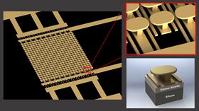
 These images show the novel semiconductor-free microelectronic device made from a gold metasurface on top of a silicon wafer with a layer of silicon dioxide in between. Images: UC San Diego Applied Electromagnetics Group.
Engineers at the University of California San Diego have fabricated the first semiconductor-free, optically-controlled microelectronic device. Using metamaterials, the engineers were able to build a microscale device that displays a 1000% increase in conductivity when activated by low voltage and a low-power laser.
This discovery paves the way for microelectronic devices that are faster and capable of handling more power, and could also lead to more efficient solar panels. The work is reported in a paper in Nature Communications.
The capabilities of microelectronic devices like transistors are ultimately limited by the properties of their constituent materials, especially the semiconductors, which can impose limits on a device's conductivity. Semiconductors have what's called a band gap, meaning they require a boost of external energy to get electrons to flow through them. And electron velocity is limited, since electrons are constantly colliding with atoms as they flow through the semiconductor.
A team of engineers in the Applied Electromagnetics Group at UC San Diego, led by electrical engineering professor Dan Sievenpiper, sought to remove these roadblocks to conductivity by replacing semiconductors with free electrons in space. "And we wanted to do this at the microscale," said Ebrahim Forati, a former postdoctoral researcher in Sievenpiper's lab and first author of the study.
However, liberating electrons from materials is challenging. It requires either applying high voltages (at least 100V), high-power lasers or extremely high temperatures (more than 1000°F), which aren't practical in micro- and nanoscale electronic devices.
To address this challenge, Sievenpiper's team fabricated a microscale device that can release electrons from a material without such extreme requirements. Their device consists of an engineered surface, called a metasurface, on top of a silicon wafer, with a layer of silicon dioxide in between. The metasurface consists of an array of gold mushroom-like nanostructures on an array of parallel gold strips.
When a low DC voltage (under 10V) and a low-power infrared laser are both applied to this gold metasurface, they generate ‘hot spots’ – spots with a high intensity electric field – that provide enough energy to pull electrons out from the metal and liberate them into space.
Tests on the device showed it could achieve a 1000% change in conductivity. "That means more available electrons for manipulation," Ebrahim said.
"This certainly won't replace all semiconductor devices, but it may be the best approach for certain specialty applications, such as very high frequencies or high power devices," Sievenpiper said.
According to the researchers, this particular metasurface was designed as a proof-of-concept. Different metasurfaces will need to be designed and optimized for different types of microelectronic devices.
"Next we need to understand how far these devices can be scaled and the limits of their performance," Sievenpiper said. The team is also exploring other uses for this technology, including photochemistry and photocatalysis, potentially leading to the development of new kinds of photovoltaic devices or environmental applications.
This story is adapted from material from the University of California San Diego, with editorial changes made by Materials Today. The views expressed in this article do not necessarily represent those of Elsevier. Link to original source.