Selective area regrowth and doping for vertical gallium nitride power devices: Materials challenges and recent progress
Volume 49, Issue , Page 296–323
| Kai Fu, Chen Yang, Hanxiao Liu, Kevin A. Hatch, Prudhvi Peri, Dinusha Herath Mudiyanselage, Bingjun Li, Tae-Hyeon Kim, Shanthan R. Alugubelli, Po-Yi Su, Daniel C. Messina, Xuguang Deng, Chi-Yin Cheng, Reza Vatan Meidanshahi, Xuanqi Huang, Hong Chen, Tsung-Han Yang, Jingan Zhou, Andrew M. Armstrong, Andrew A. Allerman, Edward T. Yu, Jung Han, Stephen M. Goodnick, David J. Smith, Robert J. Nemanich, Fernando A. Ponce, Yuji Zhao
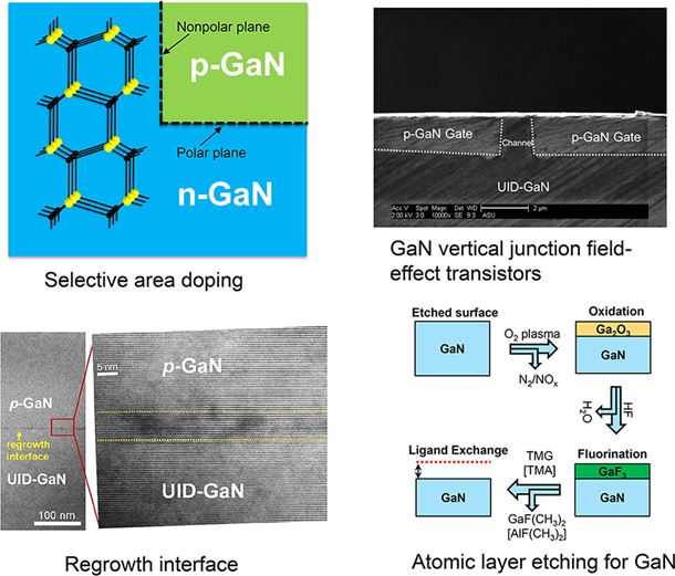
Abstract: This paper reviews materials challenges and recent progress for selective area regrowth and doping for vertical gallium nitride (GaN) power devices. The purpose is to realize randomly placed, reliable, contactable, and generally useable laterally patterned p-n junctions, which are the building blocks for various advanced power rectifiers and transistors. The general regrowth process and regrowth dynamics in trenches were discussed, where the effects of trench geometries, growth methods, and bulk substrates were elucidated. Comprehensive materials characterization techniques were utilized to analyze the regrown structures, including scanning electron microscopy, transmission electron microscopy, atom probe tomography, scanning probe microscopy, and secondary-ion mass spectrometry. Cathodoluminescence and secondary electrons in scanning electron microscopy and atom probe tomography were used to achieve lateral and vertical dopant profiling at a sub-micron scale. The regrowth interface after dry etching accumulated a high density of impurities and charges, contributing to the formation of a p+-n+ tunneling junction. This hypothesis was further confirmed by the electrostatic potential profile at the regrowth interface using electron holography. Novel etching technologies were investigated to improve the regrowth interface. It was found that low-power dry etching significantly reduced the interfacial charges and the reverse leakage currents of regrown p-n junctions. Photoelectrochemical wet etching was found to be effective in reducing deep-level defects near the regrowth interface. Atomic layer etching uses self-limiting chemical processes, thus removing the damaged layers without inducing further etching damage. Tertiarybutylchloride-based in situ etching may serve as an alternative etching method to dry etching with reduced etching damage. In terms of devices, regrown p-n junctions with low leakage currents and vertical junction field-effect transistors were demonstrated. Further improvements in selective area regrowth and associated devices can be expected using regrowth optimization and regrowth interface engineering via surface treatments and low-damage etching. These results represent an important step towards realizing selective area regrowth and doping for high performance GaN power electronics devices and systems.
Read full text on ScienceDirect
DOI: 10.1016/j.mattod.2021.04.011
Share this journal article