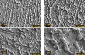
 Electron microscope images of micro- and nanostructures found on a material’s surface after application of femtosecond laser pulses. Image: Guo Lab.
Although invisible to the naked eye, tiny micro- and nanoscale structures on a material's surface can play a big role in determining that material's physical, chemical and biomedical properties. Over the past few years, Chunlei Guo and his research team at the University of Rochester have found ways to manipulate those structures by irradiating a material's surface with laser pulses. This has allowed them to alter materials to make them repel water, attract water and absorb great amounts of light – all without applying any type of coating.
Now, Guo, Anatoliy Vorobyev and Ranran Fang, researchers at the university's Institute of Optics, have advanced this research another step forward. They've developed a technique to visualize, for the first time, the complete evolution of micro- and nanoscale structural formation on a material's surface, both during and after the application of a laser pulse.
"After we determined that we could drastically alter the property of a material through creating tiny structures in its surface, the next natural step was to understand how these tiny structures were formed," Guo says. "This is very important because after you understand how they're formed you can better control them."
Having that kind of control will open the way for improvements in all kinds of technologies, including anti-corrosive building materials, energy absorbers, fuel cells, space telescopes, airplane de-icers, medical instrumentation and sanitation in third world countries.
In a paper published in Light: Science & Applications, the group introduced a scattered-light imaging technique that allows them to record the ways in which laser radiation alters a material's surface. The technique opens a window on the entire process, from the moment the laser hits the material and causes it to start melting to the formation of transient surface fluctuations to resolidification resulting in permanent micro- and nanostructures.
It currently takes about an hour to pattern a one-inch by one-inch metal sample. Identifying how micro- and nanostructures form has the potential to allow scientists to streamline the creation of these structures, increasing the speed and efficiency of such surface patterning.
Creating and altering these small structures makes properties intrinsically part of the material and reduces the need for temporary chemical coatings. To produce these effects, the researchers use a femtosecond laser, which produces an ultra-fast pulse with a duration of tens of femtoseconds. Changing the laser's conditions causes changes in the morphological features of the surface structures-- such as their geometry, size and density – leading the material to exhibit various different physical properties.
It has always proved difficult to obtain detailed images and movies of events occurring at micro- and nanoscales because they occur during a matter of nanoseconds (one billionth of a second), picoseconds (trillionths of a second) and femtoseconds (quadrillionths of a second).
To put this into perspective: Vorobyev explains that it takes about one second for light to travel from the Earth to the moon. However, light travels only about one foot in a nanosecond and approximately 0.3µm in a femtosecond, a distance comparable to the diameter of a virus or bacteria.
A typical video camera records a series of images at a rate of five to 30 frames per second. When playing the series of images in real time, human eyes perceive continuous motion rather than a series of separate frames.
So how was Guo's team able to record frames at an interval of nanoseconds, picoseconds and femtoseconds? They used a technique involving scattered light. During each femtosecond laser pulse, the beam is split in two: one beam is aimed at the material target in order to cause micro- and nanostructural change, and the second beam acts as a flashbulb to illuminate the process and record it with a CCD camera – a highly-sensitive imaging device with high-resolution capabilities.
"We worked very hard to develop this new technique," Guo says. "With the scattered light pulsing at femtosecond time intervals, we can capture the very small changes at an extremely fast speed. From these images we can clearly see how the structures start to form."
Guo explains that this scattered light visualization technique has applications for capturing any process that takes place on a minute scale. "The technique we developed is not necessarily limited to just studying the surface effects produced in my lab. The foundation we laid in this work is very important for studying ultrafast and tiny changes on a material surface." This includes studying melting, crystallography, fluid dynamics and even cell activities.
This story is adapted from material from the University of Rochester, with editorial changes made by Materials Today. The views expressed in this article do not necessarily represent those of Elsevier. Link to original source.