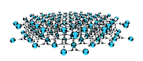
 This image shows the structure of trisodium bismuthide, with sodium atoms in white and bismuth atoms in teal. Image: FLEET.
Researchers have found that the topological material trisodium bismuthide (Na3Bi) can be manufactured to be as 'electronically smooth' as the highest-quality graphene-based alternative, while maintaining graphene's high electron mobility. They report their findings in a paper in Science Advances.
Na3Bi is a topological dirac semimetal (TDS) and considered to be a three-dimensional (3D) equivalent of graphene, because it shows the same extraordinarily high electron mobility. As with graphene, the electrons in a TDS move at constant velocity, independent of their energy.
This high electron mobility is highly desirable in materials investigated for fast-switching electronics. Theoretically, the flow of electrons in graphene can be 100 times faster than in silicon. In practice, however, there are limits to graphene's remarkable electron mobility, caused by the material's two-dimensional nature.
Although graphene itself can be extremely pure, it is far too flimsy to use as a standalone material, and so must be bound with another material. And because graphene is atomically thin, impurities in that substrate can cause electronic disorder within graphene. Such microscopic inhomogeneities, known as 'charge puddles', limit the mobility of charge carriers.
This means that graphene-based devices must be painstakingly constructed with a graphene sheet laid upon a substrate material that minimizes such electronic disorder. Hexagonal boron nitride (h-BN) is commonly used for this purpose.
Now, researchers at the Australian Research Council’s Centre of Excellence in Future Low-Energy Electronics Technologies (FLEET) have found that trisodium bismuthide (Na3Bi) grown in their labs at Monash University can be as electronically smooth as the highest-quality graphene/h-BN.
It's a significant achievement, says lead researcher Mark Edmonds. "This is the first time a 3D Dirac material has been measured in such a way. And we are excited to have found such a high degree of electronic smoothness in this material."
The discovery will be critical for advancing the study of this new topological material, which could have wide applications in electronics. "It's impossible to know how many fields of research this could open," says Edmonds. "The same finding in graphene/h-BN sparked considerable supplementary studies in 2011."
The demonstration of the electronic-smoothness of Na3Bi opens up an array of other research possibilities. There have been many studies into the relativistic (high mobility) flow of electrons in graphene since it was discovered in 2004. With this latest discovery, similar studies can now be conducted on Na3Bi, which offers several interesting advantages over graphene.
As well as avoiding the difficult construction methods involved in bi-layer graphene/h-BN devices, Na3Bi can be grown at millimeter scales or larger. Currently, graphene-h-BN is limited to only a few micrometres. Another significant advantage is the potential for using Na3Bi as the conducting channel in a new generation of transistors, building upon the science of topological insulators.
"The discovery of electronically-smooth, thin films of TDS are an important step towards switchable topological transistors," says FLEET director Michael Fuhrer.
"Graphene is a fantastic conductor, but it can't be 'switched off', or controlled," he explains. "Topological materials, such as Na3Bi, can be switched from conventional insulator to topological insulator by the application of voltage or magnetic field."
Topological insulators were recognised in last year's Nobel Prize in Physics. They are novel materials that behave as electrical insulators in their interior, but can carry a current along their edges. Unlike a conventional electrical path, such topological edge paths can carry electrical current with near-zero dissipation of energy, allowing topological transistors to act as a switch without losing energy.
Topological transistors would 'switch' just like a traditional transistor. The application of a gate potential would switch the edge paths in a Na3Bi channel between being a topological insulator ('on') and a conventional insulator ('off').
The overarching challenge is the growing amount of energy used in computation and information technology. Each time a transistor switches, a tiny amount of energy is lost as heat, and with trillions of transistors switching billions of times per second, this energy loss adds up. Already, the energy lost in computation accounts for 5% of global electricity use, and it's doubling every decade.
For many years, the energy demands of an exponentially growing number of computations was kept in check by developing ever-more efficient, and ever-more compact, computer chips – described as Moore's Law. But as fundamental physics limits are approached, Moore's Law is ending, and there are limited future efficiencies to be found.
"For computation to continue to grow, to keep up with changing demands, we need more-efficient electronics," says Fuhrer. "We need a new type of transistor that burns less energy when it switches.
"This discovery could be a step in the direction of topological transistors that transform the world of computation."
This story is adapted from material from FLEET, with editorial changes made by Materials Today. The views expressed in this article do not necessarily represent those of Elsevier. Link to original source.