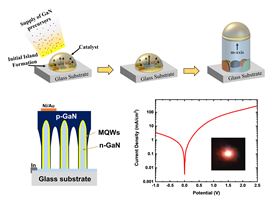
 Top: growth evolution model of GaN nanowires along m-axis; bottom left: conceptual structure of NW-based on LED on glass; bottom right: current-voltage curve with a photograph showing LED emission
With gallium nitride (GaN) showing great potential for fabricating the efficient and long lasting blue light-emitting diodes (LEDs) used in many display panels, a new study from Korea has devised a method of producing single crystalline GaN nanowire growth based on an amorphous substrate by metal-organic chemical vapor deposition (MOCVD). The breakthrough could lead to the large-scale production of a range of optical applications such as LEDs, solar cells and photodetectors, and even glass windows able to emit light or display videos.
As described in the journal Applied Materials Today [Johar et al. Appl. Mater. Today (2020) DOI: 10.1016/j.apmt.2019.100541], a team from Chonnam National University, with colleagues from the National University and the Korea Advanced Institute of Science and Technology, demonstrated for the first time the growth of universal, scalable and high crystal quality GaN nanowire-based LEDs using MOCVD on an amorphous glass substrate.
To make GaN-based LED display panels, the LEDs are required to be transferred onto a glass substrate that depends on a large amount of GaN wafers, and involves further device processing steps. Although the direct growth of GaN LEDs on glass holds potential for inexpensive and reliable LED displays, it is extremely difficult to grow single crystalline GaN on amorphous substrates. GaN is usually grown on a sapphire substrate, as it exhibits good efficiency and is long lasting but has size limitations because of its crystalline nature.
It is hoped the study will lead to growing single crystalline GaN nanowires on an amorphous substrate with uniform growth orientation, which helps the nanowires to produce highly efficient optoelectronic devices. In this growth approach, they achieved the growing of single crystalline GaN nanowires on a range of substrates, while the same approach can be used to grow other compound semiconductor nanowires on the required substrates.
As corresponding author Sang-Wan Ryu said, “The gallium nitride LED industry will particularly benefit from our growth technique especially because we can extend the upper size limit of the GaN growth area. Our approach can be used in the development of high-efficiency solar cells, LEDs on large area, cost-effective LED-based display panels.”
The team now hopes to produce the white light from GaN nanowire-based bright LEDs grown on fused silica based on enhancing the electron current channel, which is the wetting layer. In the longer term, they would like to customize ordinary glass or ITO glass for GaN nanowire-based LED fabrication, which would be dependent on lowering the GaN growth temperature and the development of a MOCVD facility scalable to such large glass substrates.
CLICK HERE TO READ THE ARTICLE IN THE JOURNAL.