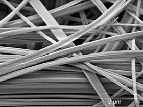
 An electron microscope image of SnIP fibers. Image: Viola Duppel/MPI for Solid State Research.
A team from the Technical University of Munich (TUM) has discovered DNA’s famous double helix structure in an inorganic material. The material is known as SnIP, for the elements tin (Sn), iodine (I) and phosphorus (P) that make it up, and is a semiconductor. However, unlike conventional inorganic semiconducting materials, it is highly flexible, producing centimeter-long fibers that can be arbitrarily bent without breaking. The material is reported in a paper in Advanced Materials.
"This property of SnIP is clearly attributable to the double helix," explains Daniela Pfister, who discovered the material and works as a researcher in the work group of Tom Nilges, professor for synthesis and characterization of innovative materials at TUM. "SnIP can be easily produced on a gram scale and is, unlike gallium arsenide, which has similar electronic characteristics, far less toxic."
The semiconducting properties of SnIP promise a wide range of application opportunities, from energy conversion in solar cells and thermoelectric elements to photocatalysts, sensors and optoelectronic elements. By doping with other elements, the electronic characteristics of the new material could be adapted for a wide range of applications.
Due to the arrangement of atoms in the form of a double helix, the fibers, which are up to a centimeter in length, can be easily split into thinner strands. The thinnest fibers produced to date comprise only five double helix strands and are just a few nanometers thick. That opens the door also to nanoelectronic applications.
"Especially the combination of interesting semiconductor properties and mechanical flexibility gives us great optimism regarding possible applications," says Nilges. "Compared to organic solar cells, we hope to achieve significantly higher stability from the inorganic materials. For example, SnIP remains stable up to around 500°C."
"Similar to carbon, where we have the three-dimensional (3D) diamond, the two dimensional (2D) graphene and the one dimensional nanotubes," he adds, "we here have, alongside the 3D semiconducting material silicon and the 2D material phosphorene, for the first time a one dimensional material – with perspectives that are every bit as exciting as carbon nanotubes."
Just as with carbon nanotubes and polymer-based printing inks, SnIP double helices can be suspended in solvents like toluene, allowing thin layers to be produced easily and cost-effectively. "But we are only at the very beginning of the materials development stage," says Pfister. "Every single process step still needs to be worked out."
Since the double helix strands of SnIP come in left- and right-handed variants, materials that comprise only one of the two should display special optical characteristics. This makes them highly interesting for optoelectronics applications. So far, however, there is no technology available for separating the two variants.
Theoretical calculations by the researchers have shown that a whole range of other elements should also form these kinds of inorganic double helices. The researchers are now working intensively on finding suitable production processes for further materials.
This story is adapted from material from the Technical University of Munich, with editorial changes made by Materials Today. The views expressed in this article do not necessarily represent those of Elsevier. Link to original source.