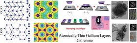
 Theoretically predicted two distinct atomic arrangements of monolayer of Ga oriented along two crystallographic (010) and (100) directions, respectively. Electron localization function (ELF) of 2% strained structure of b010 along x direction and 6% strained structures of a100, monolayers. The ELF is shown by the color bar, with red (blue) showing maxima (minima). The ELF shows uniform covalent bonding behavior in a100 gallenene and a mixture of covalent and metallic in b010 gallenene. A simple exfoliation technique of surface solid layers from the molten phase of Ga to synthesize these 2D metallic sheets is also shown. The shown transmission electron microscopy images and the theoretically predicted structures are in excellent agreement.
Researchers from Rice University, Bruker Nano Surfaces, the Indian Institute of Science and the Indian Institute of Technology have created atomically thin layers of the metal gallium on silicon substrates [Kochat et al., Sci. Adv. 4 (2018) e1701373, https://doi. org/10.1126/sciadv.1701373].
Two-dimensional materials just a few atoms thick have attracted much attention since the discovery of graphene and its unique combination of properties. Numerous other two-dimensional materials have since joined the family, such as hexagonal boron nitride and semiconducting transition metal dichalcogenides. However, two-dimensional metallic materials have proved more elusive.
Inspired by the simple exfoliation of graphene from graphite, Abhishek K. Singh, Chandra S. Tiwary, Pulickel M. Ajayan and colleagues devised a simple means of producing very thin layers of gallium, which they nickname ‘gallenene’.
“Weak interlayer forces in graphite can be utilized to separate atomically thin layers with the help of scotch tape,” explains Tiwary. “In case of solid metals, such phenomena cannot be utilized. But the solid-liquid interface is weak in metals, and we have utilized this to separate the solidified solid from the top surface.”
Atomically thin layers of gallium are exfoliated by simply dipping a Si/SiO2 substrate mounted on a diamond indenter into the molten metal. As the molten metal cools on the solid substrate, the forces between the top few atomic layers of the solidified metal and the liquid melt below are much less than within the completely solid material.
“We can utilize the surface adhesion properties of a solid with a substrate to separate a few atomically thin layers of gallium from its molten liquid,” says Tiwary.
Gallenene appears to take up two distinctive atomic arrangements, depending on the orientation during exfoliation, either retaining its usual lattice structure (gallenene b010) or taking up a honeycomb-like structure (gallenene a100) (Fig. 1). Of the two crystalline arrangements, gallenene b010 appears more stable than the other form, but both show good stability under normal, room temperature conditions.
“The novelty of our work is its simplicity and easy scalability,” says Tiwary. “We can exfoliate large-scale areas of atomically thin sheets of gallenene without the need for large amounts of energy or complicated processing parameters.”
It is early days to talk about applications of gallenene as yet, say the researchers, as no one has explored the properties of the atomically thin metal. But they envisage that metallic two-dimensional materials such as gallenene could be very useful in the construction of contacts for two-dimensional circuits and electronic devices.
“We want to understand the basic properties of the material first before we can start to explore different applications,” explains Tiwary.
This article was first published in Nano Today 20 (2018) 1-6.