Spontaneous heteroassembly of 2D semiconducting van der Waals materials in random solution phase
Volume 58, Issue , Page 18–29
| Sung Hyun Kim, Cheolmin Park, Dong-Ha Kim, Hong Ju Jung, Juhyung Jung, Hojin Lee, Panpan Li, Hongjun Kim, Seungbum Hong, Sung-Yool Choi, Il-Doo Kim, Prem Prabhakaran, Kwang-Sup Lee, Sang Ouk Kim
Abstract
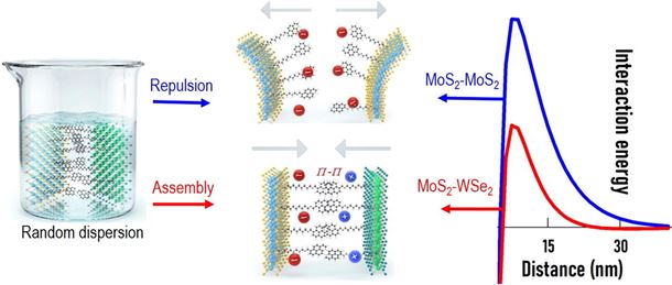
van der Waals heterostructures (vdWHs), consisting of more than one type of atomically thin 2D crystal layers are emerging platforms for interesting electrical, optical, and catalytic applications. High yield production of vdWHs with atomic scale precision is crucial prerequisite for practical utilization. Here we present a generalized approach of random solution phase, high yield heteroassembly of semiconducting vdWHs by exploiting inherent surface charge states of 2D materials as well as chemical affinity of specific ligand end-functionalities. Facile removal of noncovalent functionalized ligands via simple pH reversal enables clean interfaces within vdWHs, yielding outstanding optoelectrical and electrochemical properties driven by fluent interfacial charge transfer among the layered 2D structures. The generality of this procedure is demonstrated by the formation of a series of different vdWHs such as WSe2-MoS2, graphene–MoS2 - and phospherene–WSe2 heterostructures. Atomically thin WSe2–MoS2 phototransistor displayed an exceptionally fast response time with high sensitivity. Graphene–MoS2 overcomes the inherent charge transfer issue of MoS2 for electrochemical catalyst. Phospherene–WSe2 successfully addresses poor ambient stability of phospherene together with enhanced surface activity towards chemical sensing.
See full text for more information.
Read full text on ScienceDirect
DOI: 10.1016/j.mattod.2022.07.003
Share this journal article