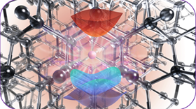
 A ball-and-stick representation of the atoms in a crystal with a spin defect in the center, and three-dimensional surfaces (red and blue) showing the excited states of the defect. Image: Peter Allen.
Researchers at the University of Chicago’s Pritzker School of Molecular Engineering (PME), Argonne National Laboratory and the University of Modena and Reggio Emilia in Italy have developed a new computational tool to describe how the atoms within quantum materials behave when they absorb and emit light. This tool, which will help scientists better understand and engineer new materials for quantum technologies, will be released as part of the open-source software package WEST.
“What we’ve done is broaden the ability of scientists to study these materials for quantum technologies,” said Giulia Galli, professor of molecular engineering at PME and senior author of a paper on this work in the Journal of Chemical Theory and Computation. “We can now study systems and properties that were really not accessible, on a large scale, in the past.”
Galli and his group showed the accuracy of the tool, known as WEST-TDDFT (Without Empty States – Time-Dependent Density Functional Theory), by using it to study three different semiconductor-based materials, but they said it can be applied to a wide range of related materials. The software they developed can also run at scale on multiple high-performance computer architectures.
The fundamental units of information underlying new, powerful quantum technologies are qubits. Unlike the bits used in classical computing, which use 0s and 1s to encode data, qubits can exist in a superposition of states, representing both 0 and 1 simultaneously.
Miniscule defects within materials – such as a missing or substituted atom in the structured lattice of a crystal – can take on quantum states and be used as qubits. These qubits are extremely sensitive to the electric, optical and magnetic properties of their surroundings, giving them the ability to be used as sensors. Understanding exactly how these ‘point defects’ interact with photons of light to change their energy states can allow researchers to manipulate them better or to design materials that use qubits as sensors or data-storage units.
“How these materials are absorbing and emitting light is critical to understanding how they are functioning for quantum applications,” said Galli. “Light is how you interrogate these materials.”
Until now, researchers could predict both the absorption and the emission of light by point defects, but they could not fully explain some of the atomic processes that happened within the material while in its excited state, especially in the case of large and complex systems.
The quantum mechanical equations that must be solved to determine the atomic properties of materials are incredibly complex and require a large amount of computing power. In this work, Galli’s team developed a new way of solving such equations more efficiently than in the past while proving that they were still accurate. The increased speed and efficiency with which the equations can now be solved means they can be applied more easily to larger systems – in the past, the computing time and power required to analyze these systems made it unfeasible.
“With these methods, we can study the interaction of light with materials in systems that are quite large, meaning that these systems are closer to the experimental systems actually being used in the laboratory,” said graduate student Yu Jin, first author of the paper.
The efficient approach developed by the team can run on two different computer architectures – central processing units (CPUs) and graphics processing units (GPUs). The researchers used the tool to study the excited state properties of point defects within three materials: diamond, 4H silicon carbide and magnesium oxide. They found that it could effectively calculate the properties of these systems, even when they comprised hundreds or thousands of atoms.
The group is continuing to apply and fine-tune the algorithms available in the package, including WEST-TDDFT, to study broad classes of materials, not only for quantum technologies but also for low-power and -energy applications.
“We’ve found a way to solve the equations describing light emission and absorption more efficiently so that they can be applicable to realistic systems,” said Govoni. “We showed that the method is both efficient and accurate.”
The new tool fits with the broader goal of the Galli lab to study and design new quantum materials. In a paper in Nano Letters, they recently reported results showing how spin defects close to the surface of a material behave differently than those deeper within a material, depending on how the surface is terminated. Their results have implications for the design of quantum sensors that rely on spin defects.
This story is adapted from material from the University of Chicago, with editorial changes made by Materials Today. The views expressed in this article do not necessarily represent those of Elsevier. Link to original source.