 An electron beam placed at a series of locations on a sheet of twisted hBN intensifies the light emission from each location. The brightness depends on how long the beam sits at a given point, or the electron flux delivered to that point. The result is an illuminated pattern. Image: Su et al. 2022.
Achieving scalability in quantum processors, sensors and networks requires novel devices that are easily manipulated between two quantum states. To this end, a team led by researchers from the US Department of Energy’s Lawrence Berkeley National Laboratory (Berkeley Lab) has developed a solid-state ‘twisted’ crystalline layered material that can give rise to tiny light-emitting points called color centers. These color centers can be switched on and off with the simple application of an external voltage.
“This is a first step toward a color-center device that engineers could build or adapt into real quantum systems,” said Shaul Aloni, a staff scientist at Berkeley Lab’s Molecular Foundry, who co-led the study. For example, the research, which is detailed in a paper in Nature Materials, could lead to a new way to make quantum bits, or qubits, which encode information in quantum computers.
Color centers are microscopic defects in a crystal, such as diamond, that usually emit bright and stable light of a specific color when activated with a laser or other energy source such as an electron beam. Their integration with waveguides, devices that guide light, can connect operations across a quantum processor.
Several years ago, researchers discovered that color centers in a synthesized material called hexagonal boron nitride (hBN), which is commonly used as a lubricant or additive for paints and cosmetics, emitted even brighter colors than the color centers in diamond. But engineers have struggled to use the material in applications because producing the defects at a determined location is difficult, and they lacked a reliable way to switch the color centers on and off.
The Berkeley Lab team has now solved these problems. Cong Su, a postdoc in the research group led by Alex Zettl, a faculty senior scientist at Berkeley Lab and professor of physics at the University of California (UC) Berkeley, examined how color centers behaved in different sophisticated forms of hBN. The team found that two stacked and twisted layers of the material resulted in the activation and enhancement of ultraviolet (UV) emission from a color center, which can be shut off when a voltage is applied across the structure.
“It’s like a sandwich with two pieces of bread, but one rotated relative to the other,” said Zettl. The rotation between the two layers stimulates the color centers at the interface to become extremely bright. The applied voltage then easily and reversibly tunes the intensity from bright to completely dark, without ‘unrotating’ the halves.
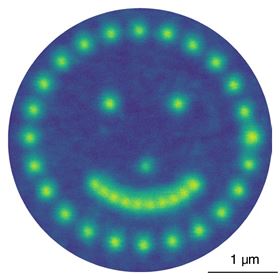
Aloni’s development of a modified electron microscope that could not only probe the material’s structure but also collect the emitted light for analysis turned out to be key for this study. This setup uses an electron beam to activate the color centers, allowing the researchers to draw patterns, such as a smiley face, onto hBN. “People typically zap the material with lasers or ions, but we’ve instead zapped it with a beam of electrons,” said Zettl.
This study achieves three steps toward the realization of a scalable quantum device. First, the UV color centers in hBN can be reliably activated to exceptional maximum brightness, by twisting the crystal interface. Second, these color centers can then be gradually and reversibly dimmed by a simple applied voltage. Finally, electron-beam treatment allows further precise spatial positioning of the color centers.
Theoretical calculations led by Steven Louie, a faculty senior scientist at Berkeley Lab and distinguished professor of physics at UC Berkeley, provided candidates for the UV color center atomic configuration to help explain why their brightness depended on the twist angle. The light emission process involves an excited electron wandering around and recombining with a hole at the color center. But a typical hBN structure has many traps that could capture the electrons, preventing light emission. “Twisting the crystal layers removes many of these traps, or ‘quantum parking lots’, near the interface,” said Louie.
The team next intends to prepare samples that allow atomic characterization, so they can pinpoint the specific atomic structures behind this mechanism and add additional levels of control. “The work is pointing us in the direction of new types of mechanisms that we can use to control the emission even better, and this is very important for many applications in quantum information sciences,” said Aloni.
This story is adapted from material from Lawrence Berkeley National Laboratory, with editorial changes made by Materials Today. The views expressed in this article do not necessarily represent those of Elsevier. Link to original source.