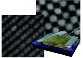
 The electron microscope images show two of the ordered structures formed in the experiments. (Bottom right) A model of the device used for measuring the electronic properties; the superlattice lies between two electrodes while an ionic gel on top (gate electrode) is used to accumulate carriers in the active material. Image: Arjen Kamp, Majid Ahmadi & Jacopo Pinna/University of Groningen.
Quantum dots are clusters of around 1000 atoms that can act as one large ‘super-atom’; their electronic properties can be controlled by just changing their size. However, to create functional devices, a large number of quantum dots have to be combined into a new material. During this process, the properties of the dots are often lost.
Now, a team of researchers led by Maria Antonietta Loi, professor of photophysics and optoelectronics at the University of Groningen in the Netherlands, has succeeded in getting quantum dots to self-assemble into a highly conductive optoelectronic metamaterial. The researchers report this work in a paper in Advanced Materials.
Quantum dots made of PbSe (lead selenide) or PbS (lead sulphide) can convert shortwave infrared light into an electrical current, which is a property that could prove useful in detectors or telecommunication switches. “However, a single dot does not make a device,” explains Loi. “And when dots are combined, the assembly often loses the unique optical properties of individual dots, or, if they do maintain them, their capacity to transport charge carriers becomes very poor. This is because it is difficult to create an ordered material from the dots.”
Working with colleagues from the Zernike Institute for Advanced Materials at the University of Groningen, Loi experimented with a method for producing a metamaterial from a colloidal solution of quantum dots. These dots, each about 5–6nm in size, show a very high conductivity when assembled in an ordered array, while maintaining their optical properties.
“We knew from the literature that dots can self-organize into a two-dimensional, ordered layer,” says Loi. “We wanted to expand this to a 3D material.” To achieve this, the researchers filled small containers with a liquid that acted as a ‘mattress’ for the colloidal quantum dots. “By injecting a small amount onto the surface of the liquid, we created a 2D material. Then, adding a bigger volume of quantum dots turned out to produce an ordered 3D material.”
Rather than being submersed in the liquid, the quantum dots self-orient on the surface to achieve a low-energy state. “The dots have a truncated cubic shape, and when they are put together, they form an ordered structure in three dimensions; a superlattice, where the dots act like atoms in a crystal,” explains Loi. This superlattice of quantum dot super-atoms displays the highest electron mobility ever reported for quantum dot assemblies.
It took special equipment to determine what the new metamaterial looks like. The team used an electron microscope with atomic resolution to study the details of the material. They also ‘imaged’ its large-scale structure using a technique called grazing-incidence small-angle X-ray scattering. “Both techniques are available at the Zernike Institute, thanks to my colleagues Bart Kooi and Giuseppe Portale, respectively, which was a great help,” says Loi.
Measurements of the electronic properties of the matematerial show that it closely resembles that of a bulk semiconductor, but with the optical properties of the quantum dots. Thus, this experiment paves the way for creating new metamaterials based on quantum dots. The sensitivity of the dots used in the present study to infrared light could be used to create optical switches for telecommunication devices. “And they might also be used in infrared detectors for night-vision and autonomous driving.”
Loi is extremely pleased with the results of the experiments. “People have been dreaming of achieving this since the 1980s. That is how long attempts have been made to assemble quantum dots into functional materials. The control of the structure and the properties we have achieved was beyond our wildest expectations.”
She is now working on understanding and improving the technology to fabricate extended superlattices from quantum dots, but is also planning to fabricate superlattices using other building blocks. “Our next step is to improve the technique in order to make the materials more perfect and fabricate photodetectors with them.”
This story is adapted from material from the University of Groningen, with editorial changes made by Materials Today. The views expressed in this article do not necessarily represent those of Elsevier. Link to original source.